Reference: Considerations to make in PCB layout
This page is intended to be a base for the creation of a new PCB layout. It is meant to be supported together with the PCB layout checklist, which is to be used in the development of the layout.
*Note: The checklist will be published when the new DMS is available however this information is still good to have.
The PCB layout is individual for each HW design. The layout is usually created in close collaboration with the selected PCB manufacturer. Depending on the knowledge and technical capabilities of the PCB manufacturer, different manufacturers are used. If you can find room for improvement, please place a process change request.
Intended for
- Hardware engineers
Overview
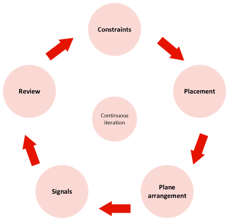
The process for the layout is iterative between the steps and you also might need to input to schematics as well. The circle below is a suggested way to start and what should be considered.
 |
|---|
| Constraints Placement Plane arrangement Signals Review |
Detailed checklist for development work
When creating a PCB layout it is recommended to use the PCB layout checklist. Below are some short motivations behind the checklist to support developers when using it. The checklist has been divided into different categories. Each category is explained in more detail in the sections below. The categories are:
- Design
- Design for manufacturing
- Documentation
- High speed design
- Impedance
- Layer stackup
- Production
- Explosion protection
Design
General considerations
- If possible, try to have components with the same CPN on the same side of the board (which makes it easier to manufacture).
- Try to keep components with a large mass on one side. Smaller components on the other side.
- Small SMT components on the bottom side need to be kept away from through-hole pins where there is selective soldering.
- Try to have connectors on one side.
- Consider test points early in the layout design.
Constraints
The input to layout design comes from the constraints given in the schematics. However, this is an iterative process so there might be cases where the layout triggers a change in the schematics.
Check solder mask
Depending on who the PCB manufacturer is and how advanced PCB designs they can create these items can be different.
- Do the openings in the solder masks have a consistent size for all pads? The size should be the same size as the copper pads or increase by for instance 50 μm. This should be consistent for all pads. If you find inconsistencies please contact your component engineer.
- If there is a component with a fine pin pitch then there might be issues in the area between pin-pads. The mask might peel off and be placed somewhere else affecting the design.
- Consider via protection before covering vias with a solder mask. Via protection
Placement
When considering how to place components on the PCBA, a good place to start is in the obstructed areas. Obstructs are areas that are setting limitations on the design. Examples of obstructs are:
- Mechanical obstructs. For instance, a connector at a certain location.
- Routing obstructs
- Component height limitations (module housing, high components on neighboring PCBs)
A suggestion is to lock obstructed areas to prevent the unintended movement of a component. For mechanical obstructs a 3D design can be imported to the design tool in order to see the items in the same view. DD (Design Description) PCB mechanical is the name of the obstruct drawing in the RACI chart on the HW process site.
Plane arrangement
Arrange the components in a way that matches the plane plan. Try to keep components with the same supply voltage in roughly the same area. Because then you can keep the supply planes local and make more use of layer space. In order to assign planes correctly consider what different supply voltages are in the design. Consider if the components are placed at the top or bottom. This is closely related to the Layer Stackup
Signals
Start by doing the layout for the power supply pins of the devices and then identify which signals are critical and which are not. These signals are identified from the constraints.
Critical Signals
- A critical signal is any signal where the overall trace length exceeds the critical length. The critical length depends on the signal rise and fall time. Please see High speed formula on critical length.
- A critical signal could be a signal that is susceptible to interference.
- A signal that has many transitions such as a clock or communication buses.
It depends on the design.
Non-critical Signals
- Signals that are slow.
- Switching events are rare. For instance a reset signal.
Design for X (DFX)
Design for X is a general term where X can be replaced with test, manufacturing, assembly, inspection etc. DFM (Design for Manufacturing) focuses mainly on the connection between the product’s physical design and its components and then improves the product design to optimize the whole manufacturing process coordinately. The adoption of DFM will shorten the product development cycle, reduce cost, and facilitate the production process. More information on Design for X
When designing there are several items impacting the material choice. The conditions that you need to meet are stated in the requirements.
- If there are any requirements indicating the restriction of use of certain components and materials for instance RoHS legislation and REACH restriction list (annex XVII).
- Material requirements come from the manufacturing documents from Industrial Engineering.
- You need to consider what is available for prototypes and for serial production. The materials may differ.
- The ambient temperature that you want to support also dictates the material choice.
- etc.
Items that increase cost
In general complexity of the design increases the cost. This is usually referred to as HDI, High Density Interconnect. A couple of examples are listed below.
- Buried vias or micro vias
- Multiple layers
- Small tolerances
Documentation
Documentation should be maintained at a level to give an easy understanding of the design in the future for maintenance. There are also formal requirements such as master-data requirements for the finalized documents. Different sites use different border styles.
High speed design
To find out what signals are considered to be high speed signals a good place to start is to check the High speed formulas
Return current
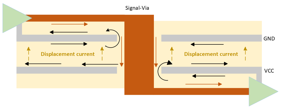
High frequency return current paths must be carefully considered and optimized to avoid signal integrity and/or EMI issues in designs with high speed digital signals. Such currents take the path of least inductance and thus will follow the same path as their corresponding signal trace on the closest reference plane. This is why any splits or voids in the reference plane must be avoided. Similar issues can arise whenever there is a layer change on a high speed signal. The following images give some examples to illustrate this:
 |  |  |
|---|---|---|
| Example 1 | Example 2 | Example 3 |
Example 1:
The image shows a driver on the top layer (i.e. L1) of a 4-layer stackup that drives a signal trace. As the input is located at the bottom side of the board, there is a via in the signal path between L1 and L4. There is also a ground plane on L2 and a VCC plane on L3.
On the outer layers, the return current takes the path of least inductance and therefore located right below the signals on their respective closest reference plane, namely L2 (GND) for the signal from the driver on L1 and L3 (VCC) for the signal to the input on L4. However, the layer transition in this example is less than ideal and here is why: whereas the signal from the driver simply follows the via, there is no similarly clear path for the return current. As a result, energy in the form of electromagnetic fields will spread out radially with respect to the via position and create dielectric displacement currents in the material between layers L3 and L2. This energy could then couple into any other signal in its path and cause signal interference (i.e. crosstalk). If such a via was located close to the edge of the board, there is also a risk of the energy leaving the PCB material and resulting in radiation issues.
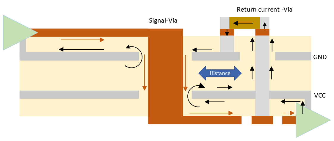
Example 2:
The overall setup is similar to example 1, however, an additional capacitor has been placed close to the signal via. This capacitor is connected to the supply planes using two additional vias. The sole purpose of this capacitor is to provide a low impedance return current path. Rather than spreading out across a large area surrounding as was the case in example 1, return currents will now use the low impedance path provided by the added capacitor to move from L3 and L2.
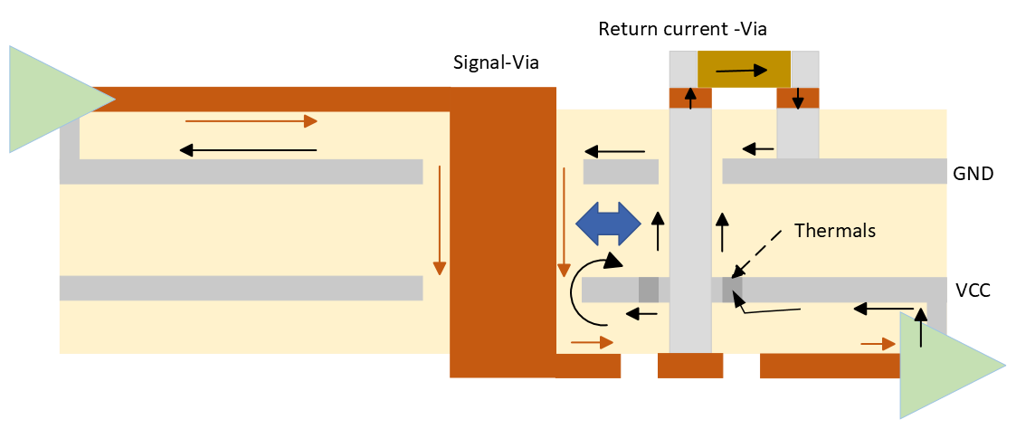
Example 3:
In this example, the vias on the capacitor have changed compared to example 2 and the longer via connecting to VCC has been moved closer to the signal via. With the signal via and the VCC via used for the return current being moved closer together, there is increased inductive coupling resulting in an overall decreased inductance (due to fields canceling each other out). This makes the arrangement in example 3 the overall better approach. In other words: it is advisable to move a signal via and a via conducting the return current as close together as possible.
Note that the approach with capacitors will not work for extremely fast signals in the multi-GHz range as the capacitors will have too much inductance at that point. In that case, layer changes should be limited to signals referencing the same plane on different sides (e.g. signal on L1, GND plane on L2, signal on L3) or between signals that both reference a GND plane with one (or more) GND vias placed close to the signal via.
Impedance
Are there impedance requirements? If so, define in which layers they are located and specify the reference planes. Define impedance values, tolerances, trace width and spacing for differential pairs. Impedance results come from the PCB manufacturer therefore to get these results the manufacturer needs to be involved when there is a layout to be able to come up with suggestions early.
 |  |
|---|---|
| Coated microstrip | Impedance in a stripline |
Simplified impedance of lossless traces
This formula (and others) can be found here: High speed formulas
Factors impacting impedance
Most software today calculates impedance using an electromagnetic field solver (examples in images field solver 1 and 2 below). Calculations by formulas are inaccurate in comparison. However, they are good to have in order to get an initial expectation of what changes will impact. Please see this example.
 |
|---|
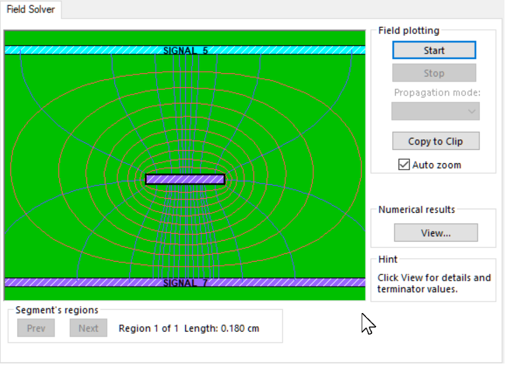
| Field Solver 1: In an actual PCB, the field distribution looks more like this (electric field in blue, magnetic field in red). You can also see how the capacitive coupling from the trace is much stronger to the lower reference plane (signal 7). However, the actual distance to the lower reference plane is only slightly smaller than that to the upper reference plane (152 µm vs 198 µm). |
 |
|---|
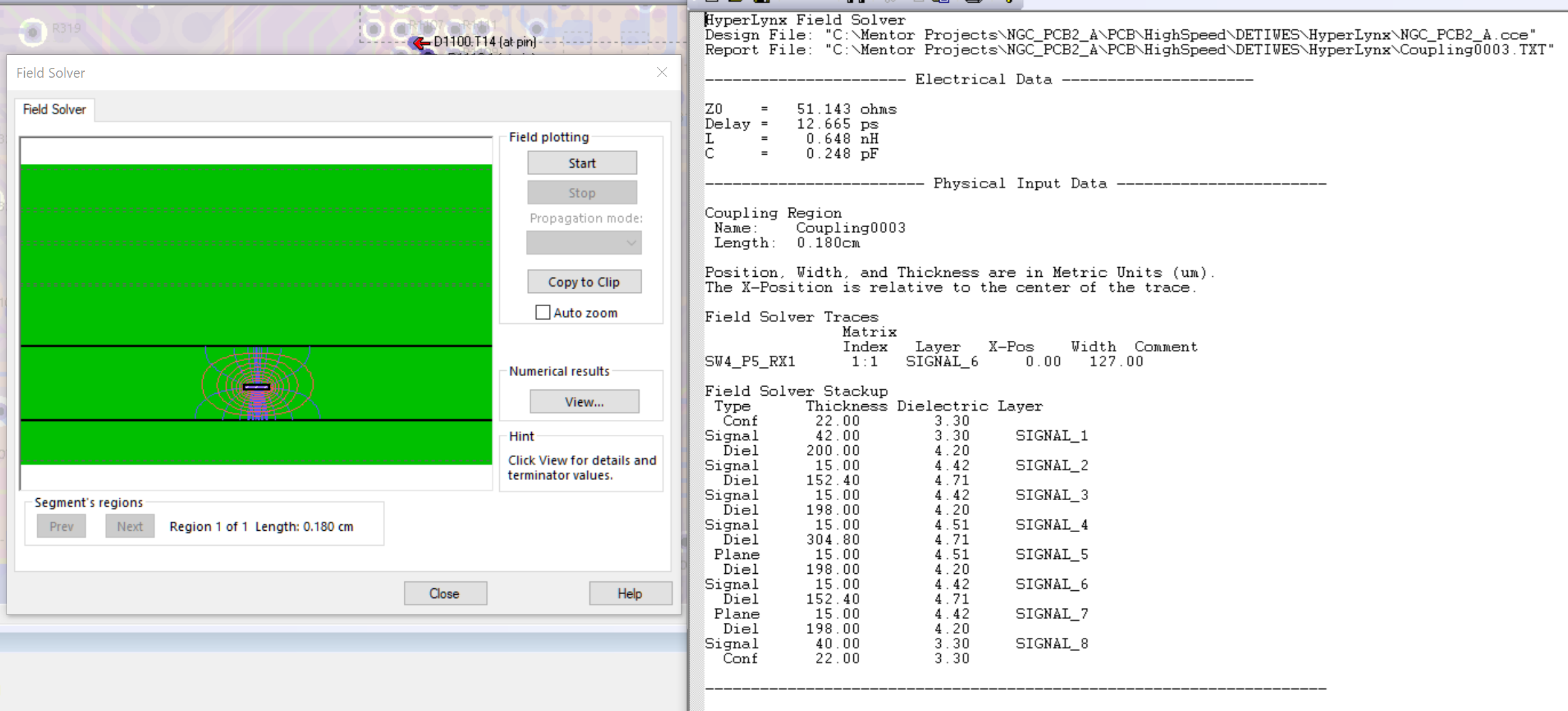
| Field Solver 2: Screenshot in Hyperlynx (electric field in blue, magnetic field in red). To show the location of the trace within the 8-layer stackup and the output of the field solver for this trace. |
Calculation with formulas example
A designer has designed a ten-layer PCB. But the conditions have changed and there needs to be two more layers added in the design. However, the overall board thickness should still be the same. If these two layers are added then they need to have the same dielectric space between them. This means that the designer will divide the dielectric layers between the copper layers. This also means that the capacitance increases. If the capacitance increases, then the impedance decreases. As the impedance decreases adjustments need to be made to maintain a higher impedance. A solution could be that traces are decreased.
For support and getting a rough estimation of how different factors affect the capacitance the below formula is a good starting point. Strictly speaking, this formula is only accurate for a plate capacitor where d << A; in such an arrangement, the electric field distribution between the plates would be uniform and very few field lines would leave the area between the plates.
 |
|---|
| Simplified image to the example above. This image is to help intuition when it comes to factors impacting impedance. |
Layer stackup
A stackup complexity is added by multiple vias and multiple layers of prepreg and core. These are individual for each design. When a stackup is set, involve the PCB manufacturer to get feedback. Early collaboration with the manufacturer reduces the risk of running into issues in production.

Via protection
Vias can be protected by for instance filling the holes before the solder mask is added. Via protection methods must be specified according to IPC4761.
Production
A tight collaboration with the PCB manufacturer is key to ensuring a smooth transition to production.
Below is an example of the gerbermachinemetric file (.txt):
    .FILETYPE GERBER_MACHINE_FILE
    .VERSION "1.0"
    .CREATOR mgerber.exe
    .DATATYPE 274X
    .DATAMODE MODAL
    .STEPMODE ABSOLUTE
    .DATAFORMAT 3 5
    .ZEROTRUNCATION LEADING
    .CHARACTERSET ASCII
    .ARCSTYLE QUADRANT
    .DELIMITER "*"
    .COMMENTS ON
    .SEQUENCENUMBERING OFF
    .UNIT MM
    .RECORDLENGTH 0
    .DEFAULTDRAWWIDTH 0.1
    .SHAPEFILLWIDTHS
    ..WIDTH 0.1
    ..WIDTH 0.2
    ..WIDTH 0.5
    ..WIDTH 1
    ..WIDTH 5
| File line | Value | Comment |
|---|---|---|
| .DATATYPE | 274X | Extended gerber |
| .DATAFORMAT | 3 5 | xxx.xxxxx |
| .ZEROTRUNCATION | LEADING | numbers on the left side of the comma are truncated |
| .UNIT | MM | states metric or imperial setting |
Suggested data viewers for production data and Gerber format:
- PCB-investigator (for both ODB++ and Gerber)
- GCprevue
Explosion protection
For designs that will be certified with for instance ATEX certification, designers need to take particular consideration to clearance and creepage distance requirements. When doing this kind of design, please involve the Ex Component responsible. For more information regarding explosion protection please see Explosion protection.
Review
For all designs, it is a good idea to have a peer review while work is in progress. When approving formal documents please follow review according to OnePCP DMS.
References
- Explosion Protection
- Industrial Engineering
- Design for X
- There are several different IPC standards that cover the aspects of the electronics industry. Mentioned on this page is IPC 4761. For more information please see the IPC standards tree. There are over 300 IPC standards.
- High speed formulas
- OnePCP DMS