FPGA Design - Methodology and VHDL-Syntax
This guide defines requirements and methodologies for VHDL designs and test benches. It helps PA develop FPGAs using VHDL.
The guide aims to ensure high quality of the developed VHDL designs so that they can be efficiently used and maintained throughout their life cycle. It also helps to provide a good and approved design methodology and design flow in each VHDL project.
It is recommended that different developers design the register-transfer level (RTL) and the test bench/case.
Note: Most code examples are incomplete and do not include headers; for example, signal and port declarations may be omitted to reduce the amount of code.
Intended for
Software engineers that work close to hardware (firmware engineers).
Design methodology and flow
FPGA design shall use a top-down design methodology. “Divide and conquer” is a beneficial mindset when implementing complicated functionality.
Using a top-down flow has several advantages.
- Complex designs can be handled more efficiently.
- Design time is reduced.
- Quality is improved.
- Reuse is facilitated.
- Automatic timing verification.
Top-down flow
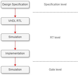
In top-down design, you first focus on specifying your circuit and then on designing it. A top-level specification is broken down into several smaller blocks that can be realized using VHDL.
Verification
Two different abstraction models must be verified in the design flow: the RTL model and the gate level/implementation. The Static Timing Analyzer must always be used to verify both.
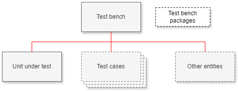
Test benches
Test benches may be designed in two ways. Stimuli and verification can be placed directly at the top level or in a separate test case. The figure below shows the structure of a test bench. The top level instantiates the unit under test (UUT), a test case (optional), and any other entities necessary to test the design. The recommendation is to use test cases for stimuli and verification.
Test benches can be divided into three different classes depending on the level of self-checking that they implement. Class 1 is the least complex, and class 3 is the most complex.
| Input stimuli | Verification of output | Timing test | |
|---|---|---|---|
| Class 1 | Test bench | Manual | Manual |
| Class 2 | Test bench | Test bench | Manual* |
| Class 3 | Test bench | Test bench | Test bench** |
*Normally recommended. **Using back annotated netlis is usually not recommended.
RTL verification
The RTL model shall be verified as follows:
-
Each hierarchical block shall be verified using a test bench (optional).
Each hierarchical level shall be verified with a test bench, which shall be written in VHDL of class 1 or 2 to quickly find simple errors in the design. -
The complete design shall be verified with a test bench.
The complete design shall be verified by using a class 2 (recommended) test bench. -
The design shall be verified in a system simulation of class 2.
A system simulation shall be performed to find more complex errors or misunderstandings of interfacing components. In the system simulation, the interfacing component shall be connected to the design. -
The designer shall spend time analyzing and trying to identify corner cases.
The designer shall “play” with the design for two to three days to find latent errors. The designer shall try to find errors by simulating the worst-case scenario in each cycle. Usually, no script shall be written in advance. The designer shall use his/her imagination in the simulation.Note: It is always advantageous if the “playing” can be documented/repeated.
Example: The designer shall activate a direct memory access (DMA) at the same time as another device wants the bus and also at the same time as the watchdog runs out and the interrupt line is activated. Then, from a design perspective, the designer shall simulate a few bus cycles and try to simulate the worst case again.
This approach is taken because generating such stimuli in a system simulation or test bench is very hard. In addition, the designer should use intuition when simulating, not a prepared script.
No functional errors shall exist after RT-level simulations (goal). This is vital, and every reasonable effort shall be made to achieve this goal. The only errors that should exist are area and timing errors, as these are handled in the implementation step. Note that if the design is asynchronous (usually not allowed), it is impossible to find all errors at this level of abstraction.
Use code coverage tools to ensure the project's coverage requirements are met. All missing lines must be explained if 100% code coverage cannot be achieved.
Gate level verification
The gate level shall be verified using a Static Timing Analyzer. The SDC file should include constraints on all data paths.
Design and methodology rules
The following section defines design and methodology rules that shall be followed in FPGA design.
Design methodology rules
The following design methodology rules apply to FPGA designs:
- A single point of definition should be considered for all source code.
- Design 100% synchronously (if possible).
- Do not copy code for reuse. Instead, store the reused code in a separate design unit or a common package (e.g., function or procedure).
- Do not use magic numbers (unique values with unexplained meanings or multiple occurrences). Constants should replace these.
- The VHDL code shall follow the syntax in this document.
- From a functional point of view, the design shall be 100% (if possible) verified at the VHDL RT level.
- The design shall be partitioned as described in the section Design partitions.
- The design shall be analyzed with a timing analyzer.
- States in the state machines should be implemented as enumerated types.
- For safety designs, all residual states in a state machine shall be handled according to the logic synthesis tool to be used.
- Effects of a state vector being forced into another state due to a single event upset should be considered (optional)
- To avoid problems with metastability, always use proper techniques when crossing clock domains, such as synchronization flip flops, handshaking, or FIFOs.
- Reset signals should be de-asserted synchronously in their respective clock domains to prevent registers from becoming metastable when reset is de-asserted.
- A script shall exist that compiles all VHDL codes for simulation automatically.
- All synthesis results (including all constraints) shall be possible to reproduce.
- All FPGAs shall use timing-driven constraints.
- Only tools and versions approved for your project may be used in your design.
- The VHDL code shall be 100% (if possible) technology independent (except IO-pad components, IP cores, and similar). Technology-dependent code shall be placed in its own entity (if possible).
- No specific tool/IP-vendor syntax is allowed in synthesizable VHDL code except for reused IP cores, IP cores from third-party vendors, or code generated by tools (e.g., Xilinx CoreGen).
- The constraints used in the synthesis tool should cover 100% of data paths.
If the rules cannot be fully complied with, the designer and the methodology responsible will discuss them and then decide.
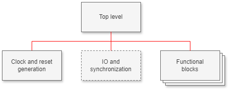
Design partitions
The FPGA shall – unless exceptional circumstances are present be partitioned in the following way:
- More than 4 hierarchical levels are not recommended.
- It is recommended that only one clock be used in each hierarchical block. This will, for example, simplify STA.
- Logic that belongs together shall be grouped in the same architecture.
- Separate very large design files into several functional hierarchies (if possible). For example, an Ethernet design can be divided into receive and transmit hierarchies. Also, try to avoid very small design files.
- Separate logic that is optimized using different optimization strategies (area/timing) (optional).
- Use structural VHDL-code (not the block command) to create hierarchies in the VHDL-code.
- Partition the functionality into processes in the design unit. Do not put everything into one huge process.
VHDL Guide
General recommendations
All VHDL code shall be written with the intent to be simulator and synthesis-independent (as far as possible). The use of non-standard constructs or supersets is not allowed. The code shall be concise. Using more code than necessary leads to lower readability and lower simulation speed. Whenever possible, unused parts of the code shall be removed.
The code shall emphasize good readability and contain a maximum of one statement per line. The TAB character shall not be used as it is environment-dependent. Related constructs shall be grouped together in a process or architecture, etc. Empty lines shall be used to increase readability. All VHDL code shall be written using lowercase characters; the exceptions are constants and generics, which are written using all uppercase.
All synthesizable VHDL code shall be compliant with VHDL-93 or VHDL 2008. Note that IP cores might violate these recommendations.
In VHDL code for synthesis, only the values ‘1’, ‘0’, ‘Z’, and ‘-‘ are allowed; the values ‘Z’ and ‘-‘ are only allowed on outputs. The use of ‘-‘ is discouraged as it can lead to simulation mismatches. If this is the case, the code must assign the value ‘1’ or ‘0’ during simulation and then change to ‘-‘ before synthesis. This must be documented in the component.
A synchronous process shall only include the clock and reset if it is asynchronous in the sensitivity list. The clock shall be the first name in the sensitivity list. The rising_edge() and falling_edge() functions should be used in synchronous processes.
Pure combinational logic is not allowed to be included in a synchronous process.
Mixing the std_logic_arith, std_logic_signed, and std_logic_unsigned packages with the numeric_std package is not recommended.
Mixing the std_logic_signed and std_logic_unsigned packages is not allowed.
Line indenting
The VHDL code shall be properly indented using space characters.
Ports in the entity declaration can be listed in the functional or directional/size grouping. Example of directional/size grouping:
inputs (bits)
inputs (vectors)
bi-directional (bits) bi-directional (vectors)
outputs (bits)
outputs (vectors)
In this case, one empty line shall be between inputs, bidirectional, and outputs. Related signals may optionally be included on the same line to reduce the length of the code.
In the functional grouping, the declarations are listed with inputs and outputs for each function, together with empty spaces, which mark the limits between groups.
The signal names, modes, and data types shall be aligned.
The code shall emphasize good readability using line indentation and empty lines where necessary.
Comments
Comments can be either in the normal flow or added to the far part of a line. When comments are in the normal flow, they start at the current indent level and should describe the code that follows it. Adding an empty line before a block comment is helpful to separate it from the code above.
When placing comments to the right of some code, keep the code neat by putting the comments in their own column – still not making lines excessively long. If a comment doesn't fit within a line, split it into two lines, where the second line only contains the comment continuation.
Comment on the declaration of all signals/parameters and also each state in a state machine.
Comments should describe design intent, not implementation. It is not necessary to comment the statement counter <= counter +1; with the comment “--Increment counter”, instead - if required - describe why the counter is being incremented.
A comment should describe all ports, signals, variables, constants, aliases, types, and each state in a state machine.
Naming conventions
Meaningful, non-cryptic identifiers based on the English language shall be used. If possible, the same identifier name as for the actual hardware and as in the datasheet or similar documentation shall be used.
All vectors shall be declared with downto so that the most significant bit is in the leftmost position (highest bit index). When interfacing to a device with bit 0 as the most significant bit, it is allowed to declare vectors with to.
Identifiers shall use alphanumeric characters, and the underscore “_” character shall be used to increase readability, e.g., load_counter. Try to keep identifier names as short as possible while still maintaining readability.
Pre- and postfixes
It is recommended that signals belonging to the same functionality share a prefix. This makes it easier to find relevant signals when, for example, simulating and allowing the use of wildcards to add signals to a wave window.
Example: All signals in a hierarchy that are used to handle a CPU interface get the prefix "cpu_" and are named
cpu_<signal_name>.
Clock signals shall use the prefix “clk_”, eg clk_cpu or clk_100mhz. Using clock names derived from the function it drives (e.g., clk_cpu instead of clk_100mhz) makes reuse easier.
Mode buffer is not allowed to be used in the entity. A “dummy” signal shall be used instead of named <port name>_b. The assignment to the output shall be first in the architecture.
If a signal needs to be synchronized, the new name shall be <signal_name>_s<1, 2, 3 …>. If only one synchronization stage is needed, the number at the end of the signal name can be omitted, e.g., cpu_addr_s.
VHDL-files and headers
All VHDL files shall be named with a .vhd extension, using all lower-case characters and “_” as a word separator, e.g., cpu_int.vhd.
Only one entity is allowed in a design file; the file shall have the same name as the entity and use the .vhd extension. Each architecture should be placed in its own design file if multiple architectures are used. In this case, architecture in the same design file as the entity is not allowed. The use of several architectures for the same entity is not recommended.
It is recommended that all synthesizable architectures be named rtl unless multiple architectures are used for the same entity.
State machines
Types of state machines
The types of state machines that shall be used are:
- Moore.
- Mealy.
- Moore with registered output.
- Mealy with registered output.
- Output = state.
State machines shall be described using one or two processes. If two processes are used, one process shall be synchronous and control state transitions, while the other can be either combinational or synchronous and control the output from each state.
Example of Moore state machine:
architecture rtl of demo_entity is
  type state_type is (s0, s1, s2, s3);     -- State declaration
  signal state : state_type;
begin

  fsm_demo_state_seq : process(clk, reset) -- Synchronous process
  begin
    if reset = '1' then
      state <= s0;                         -- Reset state
    elsif rising_edge(clk) then
      case state is
        when s0 => if in1 = '1' then
                     state <= s1;
                   end if;
        when s1 => if in1 = '0' then
                     state <= s2;
                   end if;
        when s2 => if in1 = '1' then
                     state <= s3;
                   end if;
        when s3 => if in1 = '0' then
                     state <= s0;
                   end if;
      end case;
    end if;
  end process;

  fsm_demo_output_cmb : process(state)  -- Combinatorial process
  begin
    case state is
      when s0 => out1 <= "0000";
      when s1 => out1 <= "1001";
      when s2 => out1 <= "1100";
      when s3 => out1 <= "1111";
    end case;
  end process;
Residual states
All possible states of the state vector in a state machine must be covered, including states like “0011” in a one-hot encoded state machine.
It's recommended to define what happens if you land in an undefined state by describing all residual states with when others => in the code. Note that some tools may require special modes to prevent them from optimizing away the residual state logic!
Example:
Architecture alt1 of ex is
  type state_type is (s0, s1, s2);
  signal state : state_type;
begin
  process(clk, reset_n)
  begin
    if reset_n = '0' then
      state <= s0;
      q <= '0';
    elsif rising_edge(clk) then
      case state is
        when s0 => state <= s1 ;
                   q <= '0';
        when s1 => if a = '1' then
                     state <= s2;
                   end if;
                   q <= '1';
        when s2 => state <= s0 ;
                   q <= '0';
        when others => state <= s0 ; -- Handle residual states.
                       q <= '0';
      end case;
    end if;
  end process;
end;
File structure and scripts
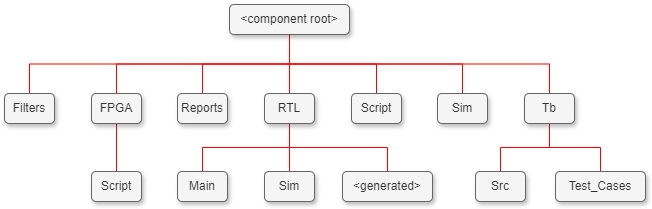
Below is an example of a file structure that can be used.
A Readme.txt and Revision.txt shall be stored at the root of the project or component ("Component root" in the below image). Readme.txt shall contain information on how to simulate and implement the design.
Example of a file structure:
 :
:
| Structure | Description |
|---|---|
| Filters | Files filter results from compilation, simulation, coverage, synthesis, and implementation. |
| FPGA/Script | Files needed to synthesize and implement the FPGA are normally only used at the top level of an FPGA. Output files from synthesis and implementation should go here. |
| Reports | Report and log files from tool runs should go here. |
| RTL/Main | Includes the synthesizable source code for the block. |
| RTL/<Generated> | This folder includes code generated by tools like Xilinx CoreGen. Its name shall represent the specific device(s) the generated code targets. |
| RTL/Sim | Includes files needed to simulate the synthesizable code (not the test bench). Normally empty. |
| Script | All scripts to verify and build the design should go here. |
| Sim | Automatically generated files from the simulation should go here |
| Tb/src | The VHDL test bench source directory. |
| Tb/Test_Cases | Test case source and simulator scripts. |
Synthesis and implementation
A script shall exist for each FPGA that runs the synthesis, map, place, and route flows and generates reports.
Other related documents
Note: This page replaces document 3BSE070754.
Please see the document management system:
- 3BSR000900 Designation of FPGAs and IPs
- 3BSE032527 FPGA Verification Methodology
- 3BSE082910 FPGA designer guide to TFS
References
- NA